Formation of the energy spectrum of electrons in a solid. Band Structure of the Energy Spectrum of Electrons
|
|||||||||||||||||||||
Band structure of the electronic energy spectrum in solids. Models of free and strongly bound electrons
3.2. Band Structure of the Energy Spectrum in the Tight-Coupling Model
3.2.1. Formation of the band structure of the energy spectrum.
So, when a bond is formed between two atoms, two molecular orbitals are formed from two atomic orbitals: bonding and loosening with different energies.
Let us now see what happens during the formation of a crystal. Here are possible two different options: when a metallic state arises when atoms approach each other and when a semiconductor or dielectric state arises.
metal condition can arise only as a result of the overlap of atomic orbitals and the formation of multicenter orbitals, leading to the complete or partial collectivization of valence electrons. Thus, a metal, based on the concept of initially bound atomic electron orbitals, can be represented as a system of positively charged ions combined into one giant molecule with a single system of multicenter molecular orbitals.
In transition and rare earth metals, in addition to the metallic bond that arises during the collectivization of electrons, there can also exist covalent directed bonds between neighboring atoms with completely filled bonding orbitals.
The collectivization of electrons, which ensures the bonding of all atoms in the lattice, leads to a 2N-fold (including spin) splitting of atomic energy levels and the formation of a band structure of the electronic energy spectrum when the atoms approach each other.
A qualitative illustration of the change in discrete energy levels of isolated atoms () with a decrease in the interatomic distance is shown in Figure 30a, which shows the splitting of energy levels with the formation of narrow energy zones containing 2N (including spin) different energy states (Fig. 30a).
 |
| Rice. thirty. |
The width of the energy bands (), as will be shown below, depends on the degree of overlap of the wave functions of the electrons of neighboring atoms or, in other words, on the probability of the transition of an electron to a neighboring atom. In general, the energy bands are separated by forbidden energy intervals, called forbidden zones(Fig. 30a).
When the s- and p-states overlap, several "bonding" and "loosening" zones are formed. From this point of view, the metallic state arises if there are zones not completely filled with electrons. However, in contrast to the weak coupling (nearly free electron model), in this case, the electronic wave functions cannot be considered as plane waves, which greatly complicates the procedure for constructing isoenergetic surfaces. The nature of the transformation of the wave functions of localized electrons into Bloch-type wave functions describing itinerant electrons is illustrated in Fig. 30b,c.
Here it should be emphasized once again that it is the collectivization of electrons, that is, their ability to move in the crystal lattice, that leads to the splitting of the energy levels of bound states and the formation of energy bands (Fig. 30c).
Semiconductor ( and dielectric) state provided by directed covalent bonds. Almost all atomic semiconductors have a diamond-type lattice, in which each pair of atoms has a covalent bond formed as a result of sp 3 hybridization [NE Kuzmenko et al., 2000]. There are two electrons on each sp 3 orbital that binds neighboring atoms, so that all bonding orbitals are completely filled.
Note that in the model of localized bonds between pairs of neighboring atoms, the formation of a crystal lattice should not lead to a splitting of the energy levels of the bonding orbitals. In fact, a single system of overlapping sp 3 -orbitals is formed in the crystal lattice, since the electron density of a pair of electrons on -bonds is concentrated not only in the region of space between atoms, but is also different from zero outside these regions. As a result of the overlap of wave functions, the energy levels of the bonding and antibonding orbitals in the crystal are split into narrow non-overlapping zones: a completely filled binding zone and a free antibonding zone located higher in energy. These zones are separated by an energy gap.
At temperatures other than zero, under the action of the energy of the thermal motion of atoms, covalent bonds can be broken, and the released electrons are transferred to the upper band on antibonding orbitals, on which the electronic states are not localized. Thus, it happens delocalization bound electrons and the formation of a certain number, depending on the temperature and band gap, itinerant electrons. Collectivized electrons can move in the crystal lattice, forming a conduction band with the corresponding dispersion law. However, now, just as in the case of transition metals, the motion of these electrons in the lattice is described not by plane traveling waves, but by more complex wave functions that take into account the wave functions of the bound electronic states.
When an electron is excited with one of the covalent bonds, hole - an empty electronic state to which a charge is attributed+q . As a result of the transition of an electron from neighboring bonds to this state, the hole disappears, but at the same time an unoccupied state appears on the neighboring bond. So the hole can move through the crystal. Just like electrons, delocalized holes form their own band spectrum with the corresponding dispersion law. In an external electric field, transitions of electrons to a free bond prevail in the direction against the field, so that holes move along the field, creating an electric current. Thus, during thermal excitation, two types of current carriers appear in semiconductors - electrons and holes. Their concentration depends on temperature, which is typical for the semiconductor type of conductivity.
Literature: [W. Harrison, 1972, ch. II, 6.7; D. G. Knorre et al., 1990; K.V. Shalimova, 1985 , 2.4; J.Ziman et al., 1972, ch.8, 1]
3.2.2. Wave function of an electron in a crystal
In the tight-binding model, the wave function of an electron in a crystal can be represented as a linear combination of atomic functions:
where r is the radius vector of the electron, r j- radius vector j th lattice atom.
Since the wave function of itinerant electrons in a crystal must have the Bloch form (2.1), the coefficient FROM _( j) for an atomic function on j-th node of the crystal lattice should have the form of a phase factor, that is,
The most valuable statement in modern physics, enough to understand all properties of solids - a hypothesis about their atomic structure .
Consider, on the basis of the atomic hypothesis, ideas about the motion of electrons in solids. It is natural to try to connect the properties of a solid with the properties of a single atom. The properties of the atom are well studied experimentally and theoretically interpreted by quantum mechanics. They can be summarized as follows.
1. An electron moving around an atomic nucleus, may be not in any condition, but only one of so-called stationary states.
2. The stationary state is characterized by a certain energy and distribution of electron density. The set of energies of stationary states forms the energy spectrum of an electron in an atom. The energy spectrum is absolutely individual for each atom, it is a kind of fingerprint. The electron density distribution shows in which areas around the atom the electron resides predominantly, that is, with a probability close to 1. The energy spectrum is usually depicted as an energy diagram (Fig. 1.1). The state with the lowest energy is called the ground state. The electron in it is closest to the nucleus.
Fig.1.1. Energy spectrum of the hydrogen atom.
The electronic properties of a crystal are determined, like the properties of an atom, by two factors - the energy spectrum of electrons in a crystal and their statistics, that is, the law of distribution over states.
The structure of the energy spectrum of a crystal can be qualitatively determined from the spectrum of an individual atom.
Imagine N identical atoms so far apart that they have no effect on each other. The energy spectrum of such an ensemble of independent atoms will consist of N matching atomic spectra. Each atomic state will simultaneously be a state of the ensemble. Such states, the energies of which coincide, are called N - multiply degenerate.
Let's start bringing the atoms together. At a certain interatomic distance, the electrostatic forces of electron-nuclear attraction and electron-electron repulsion will become noticeable. In total, attraction will prevail, but repulsion will cause the previously coinciding atomic energy levels to split into N individual levels (Fig. 1.4). When the interatomic distance is reached, a crystal is formed. Further rapprochement is hindered by large repulsive forces.
Fig.1.4. Formation of the energy spectrum of a crystal
Each atomic level is thus transformed into the zone of allowed energies of an electron in a crystal width . If the sum of half-widths of adjacent bands is less than the distance between the corresponding atomic levels, then the allowed bands are separated forbidden zone. If the sum of the half-widths exceeds the distance between the levels, then the adjacent allowed zones overlap, forming one, wider, allowed zone.
The described picture of the formation of the energy spectrum is applicable to crystals of metals, semiconductors and dielectrics. Which type a particular crystal will belong to is determined by the number of electrons Z in the atom.
If a Z is an even number, then Z/2 the lowest allowed zones will be completely filled, and the rest will be empty. The term "filled band" should be understood in the sense that there is exactly N electrons with energies belonging to a given allowed band. The uppermost of the filled bands is called the valence band, and the next empty band is called the conduction band. Crystals with such band filling are called dielectrics.
Rice. 2. Energy bands at the boundary of two semiconductors - heterostructure. Ec and E u- boundaries of the conduction and valence bands, E g is the band gap. An electron with less energy Ec 2 (level shown in red) can only be located to the right of the border
For electrons moving in a narrow-gap semiconductor and having an energy less than E c 2 , the boundary will play the role of a potential barrier. Two heterojunctions restrict the movement of an electron from two sides and, as it were, form a potential well.
In this way, quantum wells are created by placing a thin layer of semiconductor with a narrow band gap between two layers of material with a wider band gap. As a result, the electron is trapped in one direction, which leads to the quantization of the energy of the transverse motion.
At the same time, the motion of electrons in the other two directions will be free, so we can say that the electron gas in the quantum well becomes two-dimensional.
In the same way, it is possible to prepare a structure containing a quantum barrier, for which a thin layer of a semiconductor with a wide bandgap should be placed between two semiconductors with a narrow bandgap.
For the manufacture of such structures, several advanced technological processes have been developed, but the best results in the preparation of quantum structures have been achieved using the method molecular beam epitaxy.
In order to grow a thin layer of a semiconductor using this method, it is necessary to direct a stream of atoms or molecules onto a carefully cleaned substrate. Several flows of atoms, which are obtained by the evaporation of matter from separate heated sources, simultaneously fly to the substrate.
To avoid contamination, the structure is grown in a high vacuum. The whole process is controlled by a computer, the chemical composition and crystal structure of the grown layer are controlled during the growth process.
The method of molecular beam epitaxy makes it possible to grow perfect single-crystal layers with a thickness of only a few lattice periods (one crystal lattice period is about 2 ).
It is extremely important that the periods of the crystal lattices of two adjacent layers with different chemical compositions be almost the same. Then the layers will exactly follow each other and the crystal lattice of the grown structure will not contain defects.
Using the method of molecular beam epitaxy, it is possible to obtain a very sharp (up to a monolayer) boundary between two adjacent layers, and the surface is smooth at the atomic level.
Quantum structures can be grown from various materials, but the most successful pair for growing quantum wells is GaAs semiconductor - gallium arsenide and Al x Ga 1-x As solid solution, in which some of the gallium atoms are replaced by aluminum atoms. Value x is the proportion of gallium atoms replaced by aluminum atoms, usually it varies from 0.15 to 0.35. The band gap in gallium arsenide is 1.5 eV, and in the Al x Ga 1-x As solid solution it increases with increasing x. Yes, at x= 1, that is, in the AlAs compound, the band gap is 2.2 eV.
To grow a quantum well, it is necessary during growth to change the chemical composition of atoms flying to the growing layer.
First you need to grow a layer of a semiconductor with a wide bandgap, that is, Al x Ga 1-x As, then a layer of narrow-gap GaAs material, and finally again a layer of Al x Ga 1-x As.
The energy scheme of the quantum well prepared in this way is shown in Fig. 3. The well has a finite depth (several tenths of an electron volt). It contains only two discrete levels, and the wave functions at the boundary of the well do not vanish. This means that the electron can also be found outside the well, in the region where the total energy is less than the potential energy. Of course, this cannot be in classical physics, but in quantum physics it is possible.

Rice. 3. Quantum well formed in a narrow bandgap semiconductor layer sandwiched between two semiconductors with a wider bandgap
Technologists have developed several ways to obtain quantum dots and filaments. These structures can be formed, for example, at the interface between two semiconductors, where the two-dimensional electron gas is located.
This can be done by applying additional barriers that restrict the movement of electrons in one or two more directions.
Quantum filaments are formed at the lowest point of a V-shaped groove formed on a semiconductor substrate. If a semiconductor with a smaller band gap is deposited at the base of this groove, then the electrons of this semiconductor will be locked in two directions.
On fig. 4 shows quantum dots created at the interface between gallium arsenide and aluminum gallium arsenide. During growth, additional impurity atoms were introduced into the AlGaAs semiconductor. Electrons from these atoms go to the GaAs semiconductor, that is, to a region with lower energy. But they cannot go too far, as they are attracted to the impurity atoms they have left, which have received a positive charge. Almost all electrons are concentrated at the very heterointerface on the GaAs side and form a two-dimensional gas. The process of formation of quantum dots begins with the deposition of a series of masks on the AlGaAs surface, each of which has the shape of a circle. After that, deep etching is performed, during which the entire AlGaAs layer and partially the GaAs layer are removed (in Fig. 4).

Rice. four. Quantum dots formed in a two-dimensional electron gas at the interface of two semiconductors
As a result, the electrons are trapped in the resulting cylinders (in Fig. 4, the region where the electrons are located is colored red). The cylinder diameters are of the order of 500 nm.
In a quantum dot, movement is limited in three directions and the energy spectrum is completely discrete, like in an atom. Therefore, quantum dots are also called artificial atoms, although each such dot consists of thousands or even hundreds of thousands of real atoms.
The dimensions of quantum dots (one can also speak of quantum boxes) are of the order of several nanometers. Like a real atom, a quantum dot can contain one or more free electrons. If there is one electron, then it is, as it were, an artificial hydrogen atom, if two, it is a helium atom, and so on.
quantum dot- a fragment of a conductor or semiconductor, limited in all three spatial dimensions and containing conduction electrons. The point must be so small that quantum effects are significant. This is achieved if the kinetic energy of the electron ![]() , due to the uncertainty of its momentum, will be noticeably larger than all other energy scales: first of all, it is larger than the temperature expressed in energy units ( d- characteristic point size, m is the effective mass of an electron at a point).
, due to the uncertainty of its momentum, will be noticeably larger than all other energy scales: first of all, it is larger than the temperature expressed in energy units ( d- characteristic point size, m is the effective mass of an electron at a point).
quantum dot any sufficiently small piece of metal or semiconductor can serve. Historically, the first quantum dots were probably cadmium selenide CdSe microcrystals. An electron in such a microcrystal feels like an electron in a three-dimensional potential well, it has many stationary energy levels with a characteristic distance between them ![]() (the exact expression for the energy levels depends on the shape of the dot). Similar to the transition between the energy levels of an atom, a photon can be emitted during the transition between the energy levels of a quantum dot. It is also possible to throw an electron to a high energy level, and receive radiation from the transition between lower levels (luminescence). At the same time, unlike real atoms, it is easy to control the transition frequencies by changing the size of the crystal. Actually, the observation of the luminescence of cadmium selenide crystals with a luminescence frequency determined by the size of the crystal served as the first observation of quantum dots.
(the exact expression for the energy levels depends on the shape of the dot). Similar to the transition between the energy levels of an atom, a photon can be emitted during the transition between the energy levels of a quantum dot. It is also possible to throw an electron to a high energy level, and receive radiation from the transition between lower levels (luminescence). At the same time, unlike real atoms, it is easy to control the transition frequencies by changing the size of the crystal. Actually, the observation of the luminescence of cadmium selenide crystals with a luminescence frequency determined by the size of the crystal served as the first observation of quantum dots.
At present, many experiments are devoted to quantum dots formed in a two-dimensional electron gas. In a two-dimensional electron gas, the motion of electrons perpendicular to the plane is already limited, and the area on the plane can be distinguished using gate metal electrodes superimposed on the heterostructure from above. Quantum dots in a two-dimensional electron gas can be connected by tunnel contacts with other regions of the two-dimensional gas and conduction through the quantum dot can be studied. In such a system, the phenomenon of Coulomb blockade is observed.

quantum dots PbSe on PbTe layer

Rice. 1a Si 001 germanium quantum dot (scanning electron microscope photograph) (image courtesy of the HP research team)

Rice. 1b Semiconductor conical photonic channel as a quantum dot
Electrons captured by quantum dots behave just as if they were in an ordinary atom, even if the "artificial atom" does not have a nucleus. Which atom represents such a set of electrons depends on their number in the quantum dot.
 Rice. Dimensions of a nanocrystal-quantum dot
In addition to simply drawing a pattern on the surface of a semiconductor and etching it, the natural property of the material to form small islands during growth can be used to create quantum dots. Such islands can, for example, spontaneously form on the surface of a growing crystalline layer. There are other technologies for preparing quantum wells, filaments and dots, which at first glance seem very simple.
Physical bases and
And technology of electronic means
Physical foundations
E.N. VIGDOROVICH
Tutorial
"Physical Foundations"
MGUPI 2008
UDC 621.382 Approved by the Academic Council
as a teaching aid
electronic media technology
Tutorial
M. Ed. MGAPI, 2008
Edited by
prof. Ryzhikova I.V.
The textbook contains brief material on the physical foundations of the processes of formation of the properties of electronic means.
The manual is intended for teachers, engineering and technical workers and students of various specialties
______________________________
@ Moscow State Academy of Instrument Engineering and Informatics, 2005
1. ENERGY SPECTRUM OF CHARGE CARRIERS
The task before us is reduced to consideration of the properties and behavior of charged particles in a crystalline solid.
From the courses of atomic physics and quantum mechanics, the behavior of electrons in a single isolated atom is known. In this case, electrons may not have any values of energy E, but only some. The energy spectrum of electrons acquires a discrete character, as shown in Fig. 1.1 in. Transitions from one energy level to another are associated with the absorption or release of energy.
Rice. 1.1. Scheme of the formation of energy bands in crystals:
a - the arrangement of atoms in a one-dimensional crystal; b - distribution of intracrystalline potential field; in - arrangement of energy levels in an isolated atom; d - location of energy zones
The question arises of how the energy electronic levels in atoms will change if the atoms are brought closer to each other, that is, if they are condensed into a solid phase. A simplified picture of this one-dimensional crystal is shown in fig. 1.1 a.
It is not difficult to obtain a qualitative answer to this question. Consider what forces act in a single atom, and what - in a crystal. In an isolated atom, there is a force of attraction by the atomic nucleus of all their electrons and the repulsive force between electrons. In a crystal, due to the close distance between atoms, new forces arise. These are the forces of interaction between nuclei, between electrons belonging to different atoms, and between all nuclei and all electrons. Under the influence of these additional forces, the energy levels of the electrons in each of the atoms of the crystal must somehow change. Some levels will go down, others will go up on the energy scale. This is what first consequence approach of atoms. Second consequence due to the fact that the electron shells of atoms, especially the outer ones, can not only come into contact with each other, but can even overlap. As a result, an electron from one level in any of the atoms can go to the level in a neighboring atom without energy expenditure and, thus, move freely from one atom to another. In this regard, it cannot be argued that a given electron belongs to any one particular atom, on the contrary, an electron in such a situation belongs to all atoms of the crystal lattice simultaneously. In other words, it happens socialization electrons. Of course, complete socialization occurs only with those electrons that are on the outer electron shells. The closer the electron shell is to the nucleus, the stronger the nucleus holds the electron at this level and prevents the movement of electrons from one atom to another.
The combination of both consequences of the approach of atoms leads to the appearance on the energy scale, instead of individual levels, of entire energy zones (Fig. 1.1, d), i.e., regions of such energy values that an electron can have while being within a solid body. The band width should depend on the degree of bonding of the electron with the nucleus. The greater this connection, the smaller the splitting of the level, i.e., the narrower the zone. In an isolated atom, there are forbidden energy values that an electron cannot possess. It is natural to expect that something similar will be in a solid. Between zones (now no longer levels) there can be forbidden zones. Characteristically, if the distances between the levels in an individual atom are small, then the forbidden region in the crystal can disappear due to the overlap of the resulting energy bands.
In this way, the energy spectrum of electrons in a crystal has a band structure . . A quantitative solution of the problem of the spectrum of electrons in a crystal using the Schrödinger equation also leads to the conclusion that the energy spectrum of electrons in a crystal has a band structure. Intuitively, one can imagine that the difference in the properties of different crystalline substances is uniquely associated with the different structure of the electron energy spectrum (different widths of allowed and forbidden zones)
Quantum mechanics, in order to explain a number of properties of matter, considers elementary particles, including the electron, both as a particle and as a kind of wave. That is, an electron can be simultaneously characterized by the energy values E and momentum p, as well as the wavelength λ, frequency ν, and wave vector k = p/h. Wherein, Е=hν and p = h/λ. Then the movement of free electrons can be described by a plane wave, called the de Broglie wave, with a constant amplitude.
One of the main problems of solid state theory is to determine the energy spectrum and stationary states of electrons in a crystal. A qualitative representation of this spectrum can be obtained using approximate methods and simplifications. First, it is considered that the subsystem of nuclei is practically at rest (relative to the fast motion of electrons) - the adiabatic approximation. Secondly, it is assumed that each electron moves in a field created by other electrons and independent of the instantaneous position of this electron, which makes it possible to consider the motion of each electron independently of all others and describe it by the one-electron Schrödinger equation.
Such an approximation is called one-electron.
Approximation of strongly bound electrons. In an isolated atom, electrons can only occupy discrete energy levels, which are separated by intervals of forbidden energies. In this case, the electrons tend to occupy the lowest levels, but on the condition that there are no more than two electrons at each level (Pauli principle).
When a crystal is formed, due to the approach of N identical atoms, interaction forces arise between them: repulsive forces between nuclei and between electrons of neighboring atoms and extension forces between all nuclei and all electrons.
The approximation of strongly bound electrons is based on the idea that generalized electrons retain a sufficiently strong bond with atoms, and their potential energy can be represented in the following form.
 , (4.20)
where Ua is the potential energy of an electron in an isolated atom. For a crystal, it is a periodic function with a period equal to the lattice parameter, since the energy of an electron is repeated when it passes from one atom to another;  is a correction term that takes into account the influence of neighboring atoms on this energy.
If in (4.20) we neglect the correction term  ,those. consider the so-called zero approximation, then the wave function and the energy of an electron in a crystal should be taken as the wave function
  and the energy E a of an electron in an isolated atom:
  ,
, .
.
The difference between a crystal and an individual atom in this case is as follows. While in an isolated atom this energy level E a is the only one, in a crystal consisting of N atoms, it is repeated N times. In other words, each level of an isolated atom in a crystal turns out to be N-fold degenerate.
Let us now take into account the correction term  in potential energy (4.20). As the isolated atoms approach each other and form a lattice from them, each atom falls into an ever-increasing field of its neighbors with which it interacts.
In the field of these forces, the degeneracy of atomic levels is lifted. That's why every energy level, which is not degenerate in an isolated atom, splits into N close sublevels located from each other, forming an energy zone. This zone consists of very closely spaced energy levels, the density of which increases with distance from the edges of the zone according to a parabolic law, reaching a maximum in the middle of the zone. As the atoms approach, the highest energy levels split first, then, as the atoms approach, the lower ones.
The mechanism of formation of energy zones is shown in Figure 4.3.

Rice. 4.3. Scheme of the formation of energy bands in a crystal
If the energy level in an atom is (2 l+1) is a multiple degeneracy, then the energy band corresponding to it will consist of N(2 l+1) sublevels. Thus, the level s gives the zone s, consisting of N sublevels and capable of accommodating 2 N electrons: the p level gives the p band, consisting of 3 N sublevels and able to accommodate 6N electrons, etc.
Since a crystal with a volume of 1 m 3 contains approximately 10 28 atoms, and the width of the energy band is about 1 eV, the distance between the energy levels in the band is about 10–28 eV. Therefore, a negligibly small energy impact is sufficient to cause the transition of electrons from one level to another within the band; we can assume that the energy bands are quasi-continuous.
The effect of the lattice field on different levels of the atom is not the same. The levels of internal electrons that interact strongly with the nucleus experience such a weak splitting that it can be neglected: as one passes to more and more external electrons, the energy of their interaction with the nucleus decreases, and the influence of the external field increases. The strongest change under the influence of the field is experienced by the levels of external valence electrons, which are relatively weakly bound to the nucleus, and energy zones, formed from the energy levels of these electrons, appear to be the widest. This is also evidenced by the nature of the electron clouds of valence electrons: they overlap so strongly that they create the resulting cloud of almost uniform density. This corresponds to the state of their complete socialization in the grid. Such shared electrons are usually called free, and their totality is electronic gas.
The internal electrons, which are strongly bound to the nucleus, experience only a slight perturbation from neighboring atoms, as a result of which their energy levels in the crystal remain almost as narrow as in isolated atoms.
Thus, each energy level of an isolated atom in a crystal corresponds to allowed energy zone: Level 1 s – zone 1 s, level 2 R– zone 2 R etc. Zones of allowed energies are separated by areas of forbidden energies - band gaps E g. With an increase in the energy of an electron in an atom, the width of the allowed bands increases, the width of the forbidden bands decreases.
In many cases there may be an overlap of allowed zones. Like energy levels in isolated atoms, energy bands can be completely filled with electrons, partially filled and free. Everything depends on the structure of the electron shells of isolated atoms and the interatomic distances in the crystal. The uppermost of the zones, partially or completely filled with electrons, is called valence band, and the unfilled zone closest to it - conduction band.
Approximation of free electrons. Consider the case of motion of a completely free electron along the X axis, described by the following Schrödenger equation:
 , (4.21)
 , (4.22)
because a free electron has kinetic energy.
Formula (4.22) is just dispersion relation for free electrons, expressing dependence E(p). It can be converted in the following way. According to the Louis de Broglie formula,
 , (4.23)
where λ is the electron wave length, and
 . (4.24)
The vector k, coinciding in direction with the direction of propagation of the electron wave, and equal in magnitude to 2π/λ, is called wave vector of an electron. Substituting p from (4.23) into (4.22) we get
 . (4.25)
From (4.22) and (4.24) it can be seen that for free electrons the dispersion law has a quadratic character and for one-dimensional motion of an electron it is expressed by a square parabola, shown in Fig.4.4.
The solution of equation (4.21) is a plane traveling wave:
 , (4.26)
where BUT is the amplitude of the wave.

Fig.4.4. Dispersion law for a free electron
The square of the modulus of the wave function is proportional, as is known, to the probability of finding an electron in a particular region of space. As can be seen from (4.26), for a free electron this probability does not depend on the electron coordinate, since
This means that for a free electron all points in space are equivalent and the probability of finding it in any of them is the same.
Weakly bound electron approximation. Let us turn to the case of the motion of an electron in the periodic field of a crystal formed by regularly arranged lattice ions (Fig. 4.5).

Fig. 4.5. Probability of detecting an electron when moving in a field of correctly located ions
In this approximation, the potential energy of an electron is represented as
; , (4.28)
where U 0 (x) is the potential energy of an electron in the field of positive ions, assuming that this field is compensated by the field of all other electrons;
U 0 (x) - periodic function with a period equal to the lattice constant;
 - takes into account the incomplete local compensation of the ion field by electrons. The probability of finding an electron at a given location in the crystal must be a periodic function of the x coordinate, since positions that differ from each other by a multiple of the lattice constant a(for example, provisions A, A' and AT in Figure 4.5) for an electron are equally probable. Only positions within one period will be different a(for example, within the ACA' period). It means that wave function amplitude
  of an electron moving in a periodic field does not remain constant, as in a free electron, but changes periodically, or, as they say, is modulated with a period equal to the lattice period a. Let us denote this amplitude by u(x). Then the wave function for an electron moving in a periodic field crystal in the direction of the x axis, can be represented in the following form:
 , (4.29)
while u(x+na)=u(x), where n is any integer. Relation (4.29) is called Bloch function. The specific form of this function is determined by the form of the potential energy U(x) included in the Schrödinger equation (4.9).
Correspondingly, the dispersion relation for electrons moving in the periodic field of the crystal should also change in comparison with free electrons. First, the energy spectrum of such electrons acquires a band character. Inside each band, the electron energy turns out to be a periodic function of the wave vector k and for a one-dimensional crystal (atomic chain) with the parameter a can be expressed as follows:
where E a is the energy of the atomic level from which the zone was formed; FROM is the shift of this level under the action of the field of neighboring atoms; BUT- so-called exchange integral, which takes into account the possibility of transition from atom to atom that appeared in the electrons of the crystal due to the overlap of their wave functions. It is the greater, the more the wave functions overlap, i.e. the greater the frequency with which neighboring atoms can exchange their electrons. For s-states BUT s <0 , for p-states BUT p >0 , therefore it is expedient to write relation (4.30) separately for s- and p-zones:
for p-zones
where  ;
; ;
; ,
, is the absolute value of the exchange integrals for these states.
On fig. 4.6. dispersion curves are shown E(k) for s- and p-zones, construction according to equations (4.31) and (4.32).
For s-states E s at k=0
takes the minimum value  . As k increases, decreases coska and
  grows to a maximum
  at
at  .
.

Fig.4.6. Addiction E(k) in the representation of the reduced zones
Changes just the same E s (k) when it changes k from 0 before - π/а. The width of the allowed s-zone extending from E s min before E s Max, is equal to
For p-states  located at
 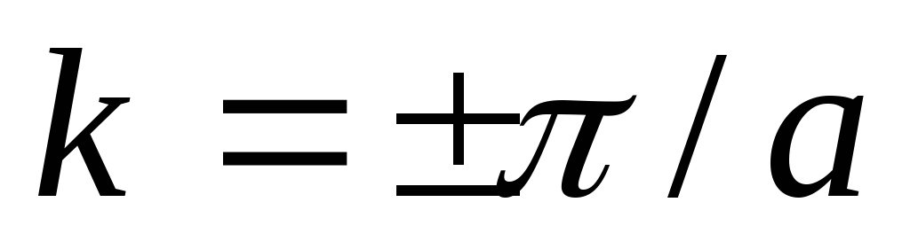 , a
, a  at k=0. p-zone width
is still determined by the value of the exchange integral А р. As a rule, the higher the atomic level is located, the more the wave functions of the electrons of this level in the crystal overlap, the larger the exchange integral, the wider the energy band formed from this level. Therefore, wide energy bands are formed from high atomic levels, separated by narrow band gaps (see Fig. 4.3).
Wave vector ranges k, within which the energy E(k)
electron, as a periodic function of k, experiences a full cycle of its change, is called Brillouin zones. For a one-dimensional crystal (atomic chain), the first Brillouin zone extends from  before
  and has a length
  (fig.4.6), two segments from
  before
  and from
  before
  represent the second Brillouin zone, etc. For values
  , where
  energy undergoes a discontinuity, leading to the formation of band gaps with a width E g .
All possible energy values in each energy zone can be obtained by changing k within the first Brillouin zone, so the dependence E(k) often built only for the first zone. All other values E can be brought into this area. This way of depicting E(k) called reduced zone diagram(fig.4.6). Another method is possible, called the extended zone scheme (Fig. 4.7).
Here, various energy zones are located in k-space in different Brillouin zones.

Fig.4.7. Depiction of energy bands in an extended band diagram
On fig. 4.7 also shows the parabolic dependence E(k)
for a free electron. Near the extrema of the dispersion curve, i.e. near points k=0
and  (middle and boundary of the first Brillouin zone),
  can be expanded into a series ka
(k are counted from 0 if the extremum is in the middle of the Brillouin zone, and from
can be expanded into a series ka
(k are counted from 0 if the extremum is in the middle of the Brillouin zone, and from  , if the extremum is on the border of the Brillouin zone) and restrict ourselves to the first two terms of the expansion:
Substituting this into (4.31) and (4.32) we get:
The minimum of the dispersion curve E(k) is called the bottom of the energy zone, maximum - summit or ceiling zones. Therefore, the obtained relations can be rewritten in the following more general form:
For the bottom of the zone;
For zone ceiling.
Thus, at the bottom and top of the energy band, the energy of an electron is proportional to the square of the wave vector, counted by the above method, and to the exchange integral, which determines the width of the band. In Figure 4.6, the parabolas corresponding to Equations 4.35 and 4.36 are shown in dotted lines.
Let us consider the physical nature of discontinuities in the energy spectrum of an electron at the boundaries of the Brillouin zones. Express k in terms of the electron wavelength λ and write down the discontinuity condition for the function E(k):
or  . (4.37)
This is the well-known Wulf-Bragg condition for an electron wave incident on a lattice perpendicular to the atomic planes. Consequently, discontinuities in the energy spectrum of an electron in a crystal occur when the Bragg reflection condition (4.37) is satisfied. Electrons with such a wavelength undergo reflection and cannot propagate in the crystal.
For real crystals, the E(k) dependence is, as a rule, much more complex than that described by formula (4.30).
On fig. 4.8. As an example, dispersion curves are given that limit the conduction band (curve 1) and the valence band (curve 2) of silicon.

Rice. 4.8. Dispersion curves and band diagram of silicon